Thin Film Physics Group

IR-Sensors
- 2-d IV-VI infrared sensor array on active Si-chip with 128 x 96 pixels
Photovoltaic Infrared Sensor: PbTe, 5 µm cut-off wavelength (See publications #183 & #184)
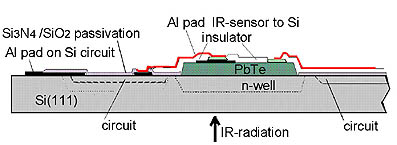
Schematic cross section of one pixel with the epitaxial PbTe IR-sensor on the active Si-substrate.
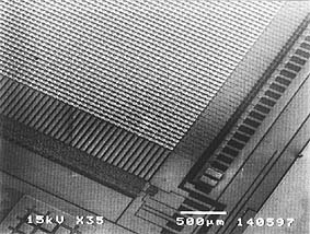
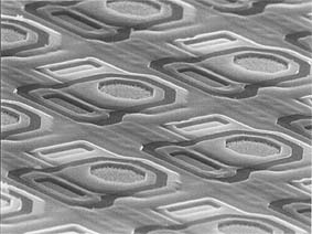
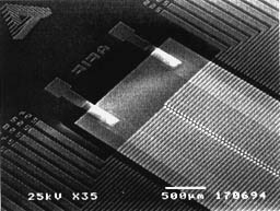
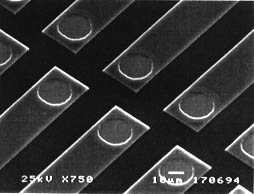
Partial view and some pixels of the completely processed epitaxial PbTe-on-Si IRFPA with the read-out electronics integrated in the Si-substrate. The Pitch is 75 µm.
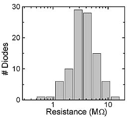
Distribution of differential resistances at zero bias (prop. to inverse noise currents) of an arbitrarily chosen line of a completely processed 96 x 128 PbTe-on-Si infrared sensor array at 95K.
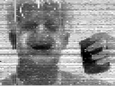
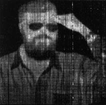
Infrared image obtained with a rudimentary demonstrational IR-camera set-up of the monolithic PbTe-on-Si array. Operation temperature is about 95K, and line integration time 100 µs. The left part of the array was bonded to a 64 channel read-out amplifier device.
- Epitaxial bilinear photovoltaic PbSnSe Infrared Sensor Array on Si with 10 µm cut-off wavelength
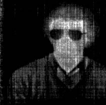
Corresponding thermal images (10 µm cut-off wavelength, Top 77K)
PbSe layer on Si:
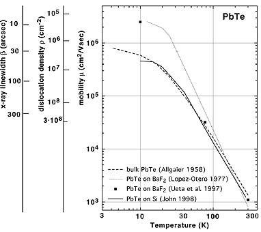
- Low temperature Hall mobilities µ as a function of threading dislocation densities r

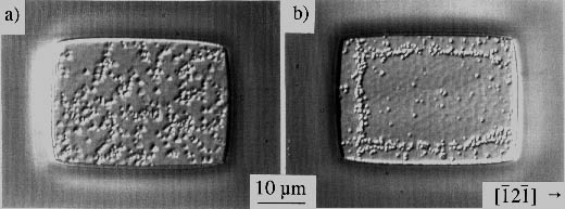
Dislocation glide in PbSnSe layers on Si(111):
- Reduction of dislocation densities by thermal cyclings to below 106 cm-2 due to thermal strains a) before, b) after thermal cycle to 300°C